electronicsforu.com /1 month ago

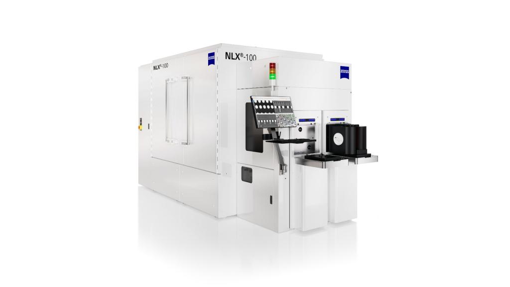
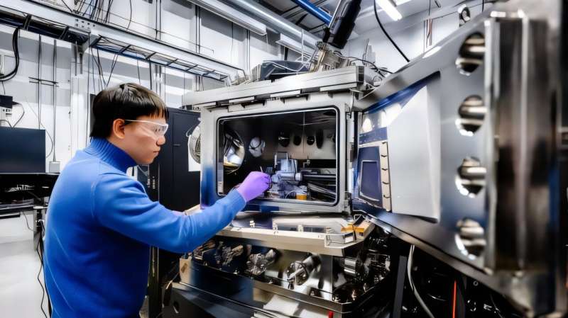
X-ray inspection reveals hidden chip defects

Can stacked chips hide defects that conventional inspection misses? Inspection and wafer correction systems target two manufacturing challenges affecting advanced semiconductor pac...
Read source
bioengineer.org /1 week ago

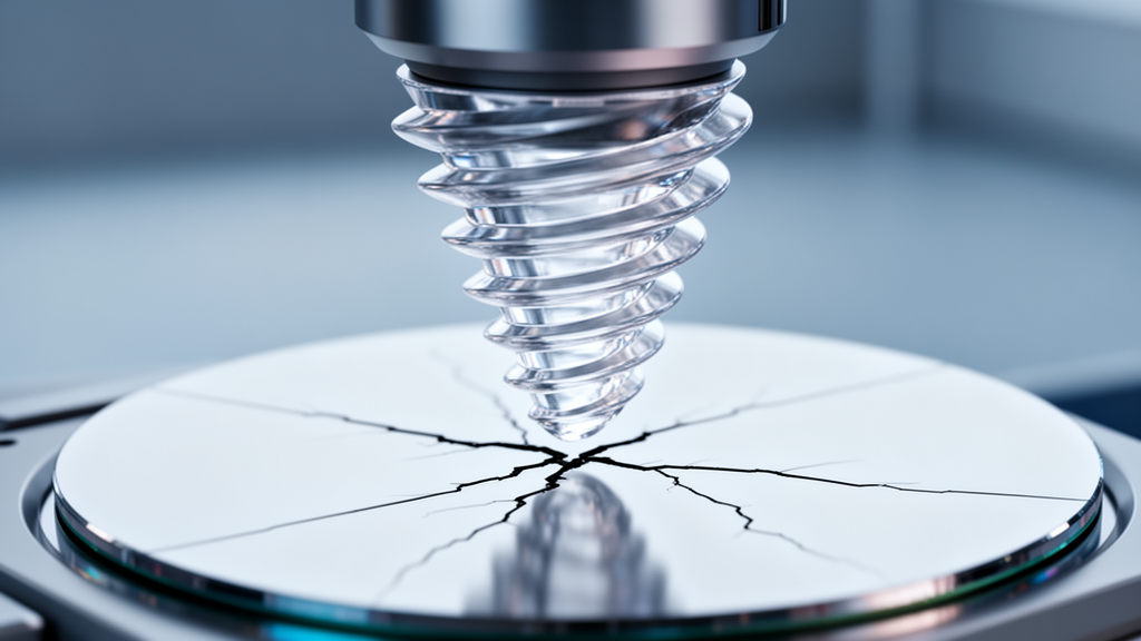
Screw Lens Ultrasound Transducer Detects Microscopic Defects in Semiconductor Chips

Researchers have developed a screw-threaded ultrasound transducer that suppresses internal lens noise to clearly reveal microscopic defects within power semiconductors.

Read source
electronicsforu.com /1 month ago

Agentic AI Automates X-Ray Inspection

Agentic AI can now guide X-ray scans of microelectronics using natural-language instructions, combining real-time image reconstruction, autonomous navigation, and AI-based feature...

Read source
qualitymag.com /1 month ago

Inspect What You Used to Pass On

BrinqAI delivers on-premises vision inspection solutions for reflective, deformable and high-variability products.

Read source
nanowerk.com /2 weeks ago

New air bearing scanner targets metrology and wafer inspection

The new A-323 scanner combines 2 g acceleration, 0.1 micron positioning accuracy and reduced vibration to improve throughput in semiconductor wafer inspection and precision metrolo...

Read source
pandaily.com /1 month ago

Xi'an Jiaotong Team Builds a Zero-Gate-Bias 2D Phototransistor to Spot Faint Grid Discharges

Gold nanoparticles and a 10nm ferroelectric gate let a WS2 device reach 1.36 x 10^14 Jones detectivity and a 9.51 ms response with no gate voltage, aimed at partial discharge monit...

Read source
electronicsforu.com /1 week ago

Infrared Cameras Bring Thermal Inspection To Production Lines

What can thermal imaging reveal that visible-light cameras miss? These industrial cameras can help manufacturers monitor temperature patterns and identify heat-related defects duri...

Read source
electronicsforu.com /1 month ago

Packaging Tools Target Larger Semiconductor Panels

Can panel-level packaging scale without compromising yield? New dispensing and plasma systems address warpage, surface preparation, and process consistency. Nordson Electronics Sol...

Read source
electronicsforu.com /5 days ago

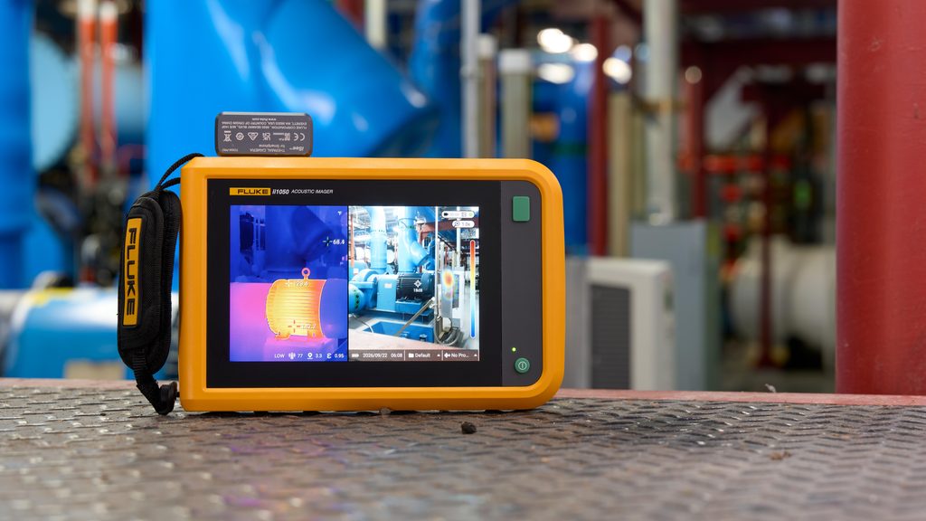
Acoustic Imagers Make Industrial Inspections Easier

How can maintenance teams detect equipment problems before they cause downtime? Improved acoustic detection and on-device reporting aim to make inspections faster and more precise....

Read source
electronicsforu.com /1 month ago

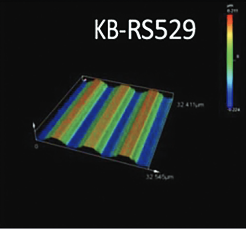
A Method To Check Metal Foil Surfaces

A test method defines procedures to measure metal foil surfaces using laser imaging, calibration, sample preparation and surface parameters. The High Density Packaging User Group (...

Read source
qualitymag.com /1 month ago

Mitutoyo Strengthens Commitment to Semiconductor Manufacturing with New Competence Center in Europe's Silicon Saxony

Mitutoyo, a global leader in precision measurement and metrology, is strengthening its commitment to the semiconductor industry with the opening of a new Semiconductor Competence C...

Read source
qualitydigest.com /1 month ago

AI Image Processing for High-Gloss Components in Quality Control

AI Image Processing for High-Gloss Components in Quality Control When glare obscures the view Mark Hembree Wed, 10/07/2026 - 12:03...

Read source
roboticsandautomationnews.com /3 weeks ago

Siemens and Nvidia advance AI-powered PCB inspection from digital twin to factory

Siemens is collaborating with Nvidia to develop adaptive AI-powered manufacturing capabilities that combine industrial software, Siemens’ Digital Twin technology and Nvidia Cosmos...

Read source
prweb.com /1 month ago

Custom Ultrasonic Transducers Address Critical Challenges in Modern Semiconductor Fabrication

As semiconductor fabs push toward smaller, denser chip designs, demand is rising for custom high-power ultrasonic transducer manufacturers capable of maintaining wafer-cleaning pre...

Read source
thequantuminsider.com /3 weeks ago

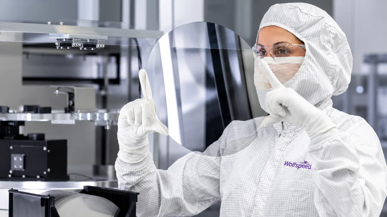
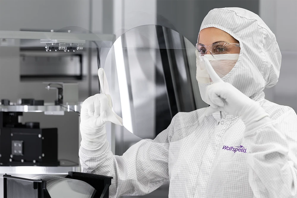
Wolfspeed Introduces Optical-Grade Silicon Carbide for Augmented Reality and Quantum Computing

Insider Brief PRESS RELEASE — Wolfspeed, Inc. (NYSE: WOLF), a global leader in silicon carbide (SiC) technology, today announced the commercial introduction of its proprietary tr...

Read source
electronicsforu.com /2 weeks ago

JOB: Field Services Engineer (Semiconductors) At Matellio India Pvt. Ltd. In Jodhpur

APPLY HERE ON LINKEDIN Location: Jodhpur Company: Matellio India Pvt. Ltd. The Engineer Level 2 will execute advanced installations, repairs, preventive maintenance, and system opt...

Read source
newswire.com /1 month ago

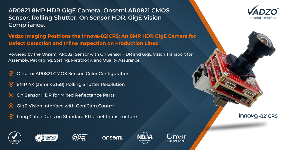
Vadzo Imaging Positions Innova-821CRS Onsemi AR0821 8MP HDR Gigabit Ethernet Camera for Industrial Inspection

The Innova-821CRS is an AR0821 HDR Gigabit Ethernet Camera built around the onsemi AR0821 sensor, delivering 8MP 4K resolution and HDR imaging for industrial inspection application...

Read source
quantumcomputingreport.com /3 weeks ago

Wolfspeed Commercializes Transparent Silicon Carbide Substrates for Quantum Computing and Integrated Photonics

Wolfspeed has launched transparent silicon carbide (TSiCâ„¢) wafers for quantum computing and integrated photonics, available in 150mm and 200mm sizes, with 300mm in sampling. This...

Read source
qualitymag.com /1 month ago

DeGould Vehicle Inspection Tech

A new AI powered drive-through vehicle inspection system designed to extend vehicle inspections beyond the factory and across the wider automotive supply chain will be deployed for...

Read source
electronicsforu.com /1 month ago

India Is Building Fabs. Who Will Build the Systems That Keep Them Running?

As semiconductor projects move towards more demanding technologies, infrastructure complexity is rising sharply. Deerns is focusing on the less visible engineering challenges, from...

Read source
qualitymag.com /1 month ago

Precision You Can See

High-precision vision system featuring parfocal zoom optics, LED profile/surface illumination, video edge detection, digital overlays and geometric functions.

Read source
qualitymag.com /1 week ago

When an Aerospace Component Fails, Where Should You Look First?

From microscopic defects to surface contamination, aerospace failure analysis requires the right tools at the right time. Explore how advanced microscopy and automation help labora...

Read source
built.itmedia.co.jp /1 month ago

スマホで撮るだけで、0.1ミリ単位のひび割れを測る「フォトノギス」

TTESは、インフラ点検DXのツールとして、貼り付けた2枚のプレート間の間隔の変化を測定する「フォトノギス」を訴求している。2枚のプレート間をスマホやデジカメで撮影するだけで、橋梁やトンネ...

Read source
qualitymag.com /1 month ago

Beyond Pass/Fail: The Shift from Defect Detection to Visual Reasoning

Visual inspection is changing. For years, a typical machine vision application was relatively static: position a camera, capture an image, analyze it and make a pass/fail decision.

Read source

Turn fresh research into a full content calendar

Use SocialBu to discover ideas, generate post drafts, and schedule them across your social channels.