electronicsforu.com
/1 week ago
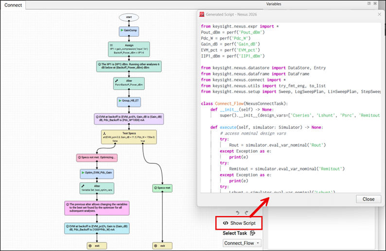
Do Chip Designers Still Need Traditional EDA Tools?
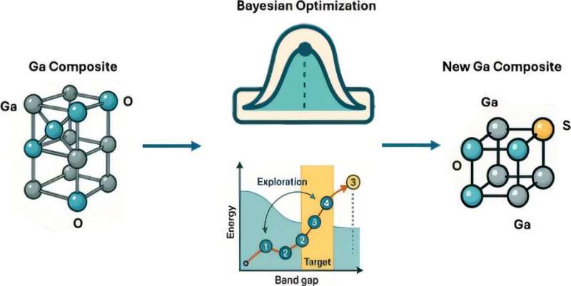
Beyond fabs, this startup is tackling a hidden semiconductor challenge that could redefine chip design and expand opportunities for innovation. India’s semiconductor ambitions are...